Scanning tunneling microscope
|
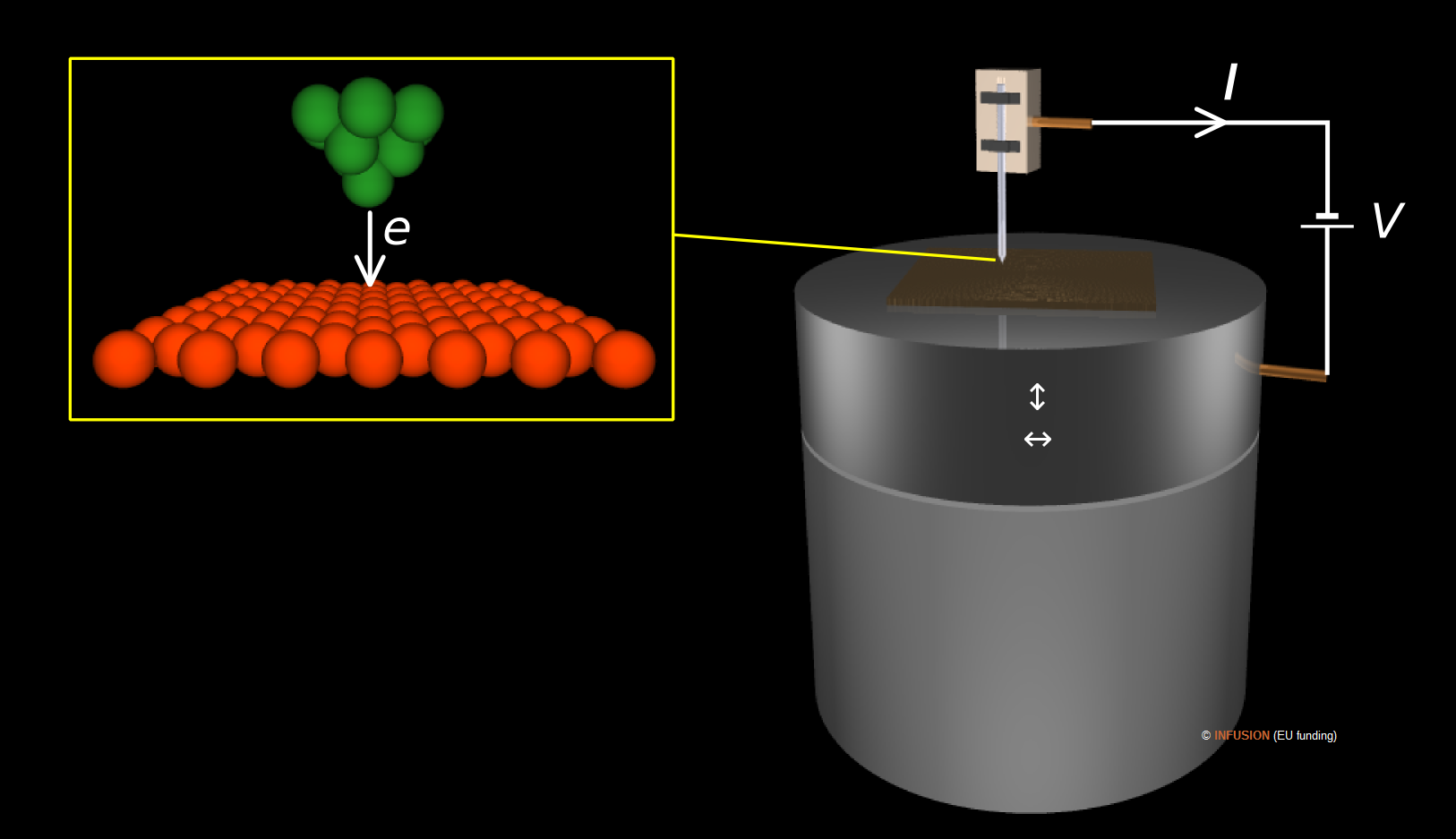
The Scanning Tunneling Microscope (STM) is one of the most important instrument in nanotechnology. STM is used to image the atoms at the surface of an atomically flat conducting sample. Moreover, it can be used to manipulate atoms, sometimes one by one. Its working principle is based on the quantum mechanical tunnel effect. The instrument has a sharp metallic tip placed nearby the surface of the sample and put at a different electric potential than the sample. The air spacing between the sample and the tip is a potential barrier a current can go through by tunnel effect, provided the barrier thickness does not exceed 1 nm. The tunnel current decreases indeed exponentially with the thickness of the barrier. Because of that dependence, it makes a difference on the tunnel current intensity if the atom located at the very end of the tip lies right above an atom of the surface or not. By moving laterally the sample in front of the tip, one obtains a signal that contains information on the atomic corrugation of the surface. |
 |
In the constant-current mode, the tunnel current is kept constant by varying the tip--sample distance while scanning the surface. The image obtained is a map of the vertical distance variations. The fine tuning of the position of the sample relative to the tip is realized by piezoelectric devices controlled by a computer. With a sharp tip, the lateral resolution of an STM can be sub-nanometer whereas its vertical resolution is sub-Angström.
 |
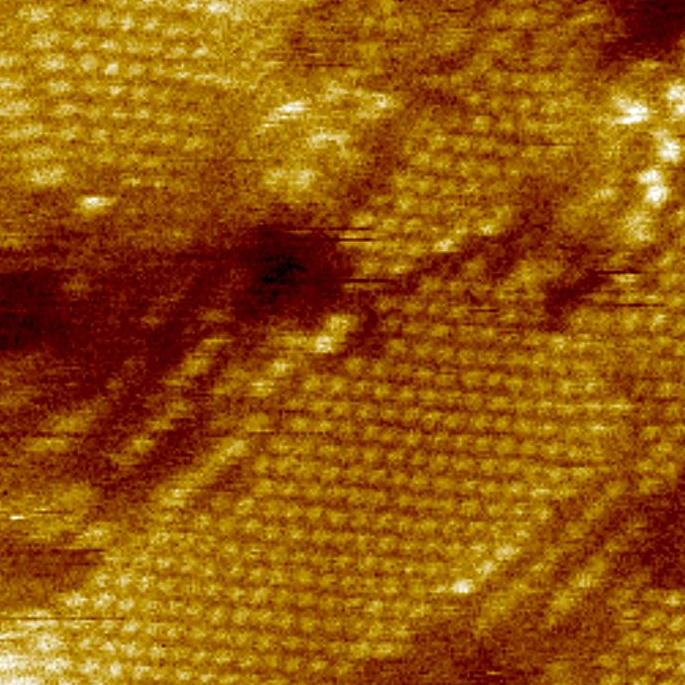
The picture is a topographic image of a self-assembled molecular layer of hydrocarbon chains, containing 8 carbon atoms and ending with a thiol group (octanethiol molecules), adsorbed on a gold layer, itself evaporated on mica (by courtesy of Prof. A. Cornia, Chemistry Department University of Modena, image obtained with a pA-STM of A.P.E. Research S.R.L.). |
An STM can be used for Scanning Tunneling Spectroscopy (STS). In this mode, the tip is located at a specific position over the surface while recording a a current--voltage I--V characteristics by varying the voltage difference between tip and sample continuously. The first derivative dI/dV provides information on the local electronic density of states of the surface.