Introduction
Nanotechnology aims at building devices in a bottom-up manner. Ultimately, this means starting from atoms or molecules and assembling them in a controlled and predefined way. Special tools exist to manipulate and characterize nanoscopic objects. Scanning tunneling microscopy (STM), atomic force microscopy (AFM), high-resolution transmission microscopy (HRTEM) are among them. These tools can only by used in the laboratory for exploratory purposes. Nanotechnology indeed requires much faster processes, including self-assembly. Here, inter-molecular interactions are exploited to put molecules and nanostructures at the right place.
 |
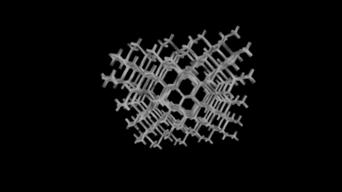
Nanostructures are atomic or molecular assemblies with size along at least one dimension below a few tens on nanometers. Atomic clusters can have a few nanometer size in the three directions. They are often called quantum dots, for the energy levels of the electrons in these tiny structures are governed by the rules of quantum mechanics. The picture illustrates a diamond nanocrystal characterized by bonds meeting along tetrahedral directions with angles of 109°. Most of the bonds are located at the surface, because the surface to volume ratio is high in a quantum dot. In the drawing, the length of the surface bonds are divided by two. In a real nanocrystal, the surface danging bonds will be saturated with hydrogen and other atoms or molecular groups. |
At the European level, the consortium called NFAA-Europe (Nanoscience foundries and fine analysis) provides access to state-of-the-art tools for multidisciplinary research at the nanoscale. The available techniques include growth and synthesis, lithography and patterning, nanocharacterization, theory and numerical simulation.