Transition metal dichalcogenides
Transition metal dichalcogenides (TMDCs), with chemical formula XZ2, are sulfides or selenides (symbol Z) of transition metals (symbol X). Like graphene, they are layered materials than can be isolated in the form of two-dimensional compounds, either by exfoliation or by direct synthesis. Monolayer TDMCs form a 2D hexagonal crystal, with lattice parameter between 0.31 and 0.40 nm (depending on the metal and the chalcogen) and a thickness of 0.6 to 0.7 nm. If some TMDCs are metallic, most are semiconductors. In the monolayer form, the band gap can be direct, in remarkable contrast with the indirect band gap realized in the bulk. This characteristics make these 2D materials suitable for optoelectronics and photovoltaics, among other applications [1].
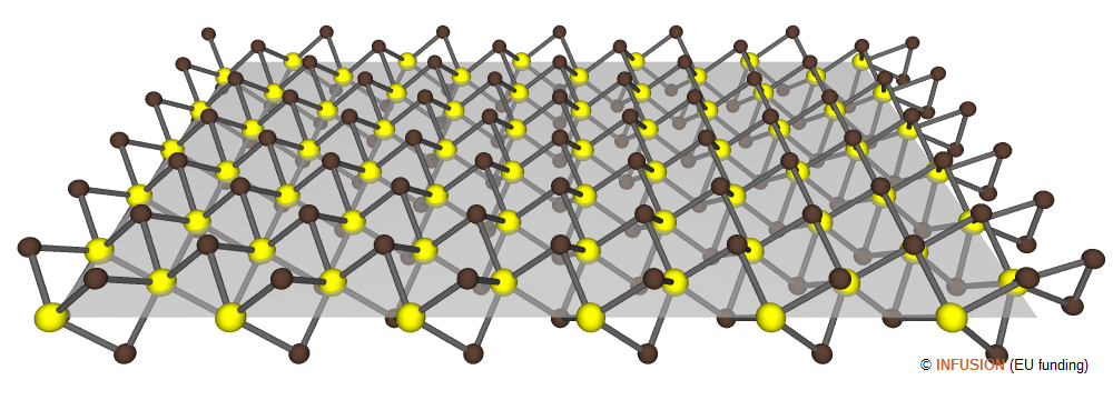 |
Ball-and-stick model of a monolayer MoS2 nanoribbon. The Mo atoms (yellow) form a triangular lattice with parameter 0.316 nm. The Mo lattice is sandwiched between two S (brown) planes mirror symmetric of each other. Each sulfur atom is connected to three Mo. Taking into account the van der Waals radius of the S atoms, the thickness of a monolayer MoS2 is 0.67 nm. In the structure illustrated here, the Mo atoms on the Mo edge of the nanoribbon are saturated by S dimers (right-hand side of the drawing). |
The following table lists the band gap of monolayer TMDCs either measured by photoluminescence (optical gap) or by STS (electronic gap) [2]. The difference between the two gaps represents the binding energy of the electron--hole pair (exciton) created by the absorption of a photon.
| TMDC | Optical gap (eV) | Electronic gap (eV) |
|---|---|---|
| MoS2 | 1.93 | 2.15 |
| WS2 | 1.95 | 2.38 |
| MoSe2 | 1.66 | 2.16 |
| WSe2 | 1.64 | 2.08 |
One of the interests of monolayer MoS2 comes from its photoluminescence properties caused by direct transitions across the gap. The photoluminescence spectrum is composed of two major peaks located at 1.85 eV (670 nm) and 2.05 eV (605 nm). The presence of two peaks is attributed to the splitting of the valence band produced by spin-orbit coupling. The intensity of the emitted light can be increased by p-type chemical doping [3]. Monolayer MoSe2 and WSe2 also present photoluminescence emission in the form of an asymmetric preak with maximum at 1.57 eV (790 nm) and 1.65 eV (751 nm), respectively. By comparison, the photoluminescence spectrum of monolayer WS2 is more symmetric with maximum at 1.97 eV (629 nm). In all these TMDCs, the photoluminescence response rapidly decreases with increasing the number of molecular layers.
- "2D transition metal dichalcogenides" S. Manzeli, D. Ovchinnikov, D. Pasquier, O.V. Yazyev, and A. Kis, Nature Rev. Mater. 2 (2017) 17033 [DOI: 10.1038/natrevmats.2017.33].
- "Electronic structures and theoretical modelling of two-dimensional group-VIB transition metal dichalcogenides" G.B. Liu, D. Xia, Y. Yao, X. Zu, and W. Yao, Chem. Soc. Rev. 44 (2015) 2643-2463 [DOI: 10.1039/C4CS00301B].
- "Tunable photoluminescence of monolayer MoS2 via chemical doping" S. Mouri, Y. Miyauchi, and K. Matsuda, Nano Lett. 13 (2013) 5944-5948 [DOI: 10.1021/nl403036h]. .